
Raytheon RF Components
362 Lowell Street
Andover, MA 01810
Revised February 6, 2003
Page 1
www.raytheonrf.com
Specifications are based on most current or latest revision.
PRODUCT INFORMATION
RMPA1951-102
3V PCS CDMA Power Amplifier Module
RF Components
Description
!
Advanced DC power-management extends average phone-
battery life!
!
Single positive-supply operation and power-down mode
!
35% power-added efficiency at +29 dBm CDMA average output
power
!
Compact LCC package: 6.0 x 6.0 x 1.5 mm
!
50 ohm matched and DC blocked input/output
Features
The RMPA1951-102 is a small-outline, power amplifier module (PAM) for CDMA Personal
Communication System (PCS) and Wireless Local Loop (WLL) applications. Advanced DC power
management provides an effective means to reduce current consumption during peak phone
usage at backed-off RF power levels. Analog or digital bias control enables the handset designer to
optimize gain, linearity and power-added efficiency over a wide range of output powers, depending on
the power-density profile of the wireless network. High power-added efficiency and excellent linearity
are achieved using Raytheon RF Components' Heterojunction Bipolar Transistor (HBT) process.
Electrical
Characteristics
3
Parameter
Min
Typ
Max
Unit
Operating Frequency
1850
1910 MHz
Gain
(Po=0 dBm)
20
24
dB
(Po=28 dBm)
25
27
dB
Linear Output Power
29
dBm
Power-Added Efficiency
(Po=16 dBm)
5
6.5
%
(Po=28 dBm)
28
32
%
(Po=29 dBm)
31
35
%
ACPR (Offset
1.25 MHz)
4
-49
-46
dBc
Noise Figure
5
6
dB
Noise Power (Po
29 dBm)
-135 dBm/Hz
Input VSWR (50
)
2.0:1
2.5:1
Output VSWR (50
)
3.5:1
Parameter
Min
Typ
Max
Unit
Stability (All spurious)
5
-70
dBc
Harmonics (Po
29 dBm)
2fo, 3fo, 4fo
-30
dBc
Quiescent Current
(Vref=2.7V)
80
100
mA
(Vref=2.0V)
50
mA
(Vref=1.7V)
35
mA
Power Shutdown Current
6
2
10
uA
Vcc
3.0
3.5
4.5
V
Vref
1.7
2.7
3.2
V
Iref
13
mA
Case Operating
Temperature
-30
+85
∞C
Notes:
1. No permanent damage with only one parameter set at extreme limit. Other parameters set to typical values.
2. Typical RF input power for CDMA Pout = +28 dBm.
3. All parameters met at Tc =+25∞C, Vcc =+3.5V, Vref=+2.7V, f=1880 MHz and load VSWR
1.2:1.
4. Po
28 dBm at Vcc=3.5V; CDMA W aveform measured using the ratio of average power within a
1.23 MHz channel to average power within a 30 kHz bandwidth at + 1.25 MHz offset.
5. Load VSWR
6:1, all phase angles.
6. No applied RF signal. Vcc=+3.5V nominal, Vref=+0.2V maximum.
Absolute
Ratings
1
Parameter
Symbol
Value
Units
Supply Voltage
Vcc
6
V
Reference Voltage
Vref
1.5 to 4.0
V
RF Input Power
2
P
in
+7
dBm
Load VSWR
V
SW R
Case Operating Temperature
T
c
-40 to +110
∞
C
Storage Temperature
T
stg
-55 to +150
∞
C
Raytheon RF Components
362 Lowell Street
Andover, MA 01810
Revised February 6, 2003
Page 2
www.raytheonrf.com
Specifications are based on most current or latest revision.
PRODUCT INFORMATION
RMPA1951-102
3V PCS CDMA Power Amplifier Module
RF Components
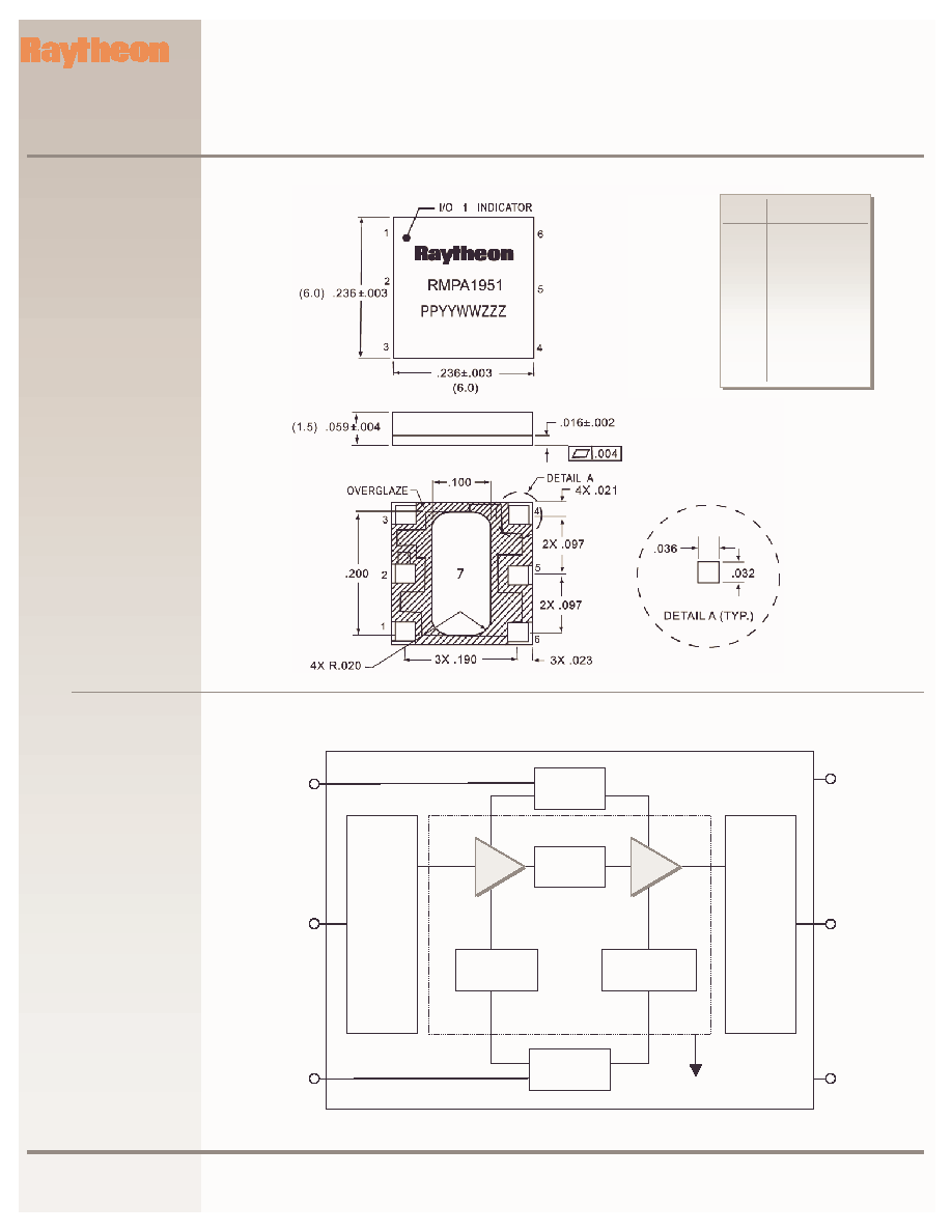
Figure 1
Package Outline and
Pin Designations
Figure 2
Functional Block
Diagram of
Packaged Product
VCC=3.5V
(nom)
VREF=2.7V
(nom) 1850-
1910 MHz
50 Ohms I/O
N/C
(4)
Input
Stage
Output
Stage
Output Stage
Bias
Input Stage
Bias
MMIC
PA Module
GND (Pin 7)-
(Package Base)
RF OUT
(5)
VCC
(1)
RF IN
(2)
VREF
(3)
GND
(6)
Interstage
Match
Collector
Bias
(Topside View)
Input
Matching
Network
Output
Matching
Network
Reference
Adjust
Dimensions in inches
(mm)
Vcc
RF In
VREF
N/C
RF Out
GND
GND
1
2
3
4
5
6
7
Descriptio
n
Pin
#
(5.08)
(2.46)
(2.54)
(4.82)

Raytheon RF Components
362 Lowell Street
Andover, MA 01810
Revised February 6, 2003
Page 3
www.raytheonrf.com
Specifications are based on most current or latest revision.
PRODUCT INFORMATION
RMPA1951-102
3V PCS CDMA Power Amplifier Module
RF Components
With device marking oriented right side up, RF IN is on the left and RF OUT is on the right.
Blue wire is collector DC voltage input (pin 1). VCC= +3.5V nominal.
Brown wire is reference DC voltage input
(pin 3).
Vref=+ 2.7V nominal to obtain Iccq= 80mA.
Operation at lower or higher quiescent currents can be achieved by decreasing or increasing Vref
voltage relative to +2.7V.
First apply +3.5V to the collector supply (blue wire). Next apply +2.7V to the reference supply to brown
wire. Quiescent collector current with no RF applied will be about 80 mA. Reference supply current with
or without RF applied will be about 13 mA. When turning amplifier off, reverse power supply sequence.
Apply -20dBm RF input power at PCS frequency (1850 -1910MHz). After making any initial small signal
measurements at this drive level, input power may be increased up to a maximum of +6dBm for large
signal, single-tone or digital CDMA measurements. Do not exceed +6dBm input power.
Evaluation
Board
Instructions
Figure 3
Evaluation Board
Layout and
Schematic
2
3
4
5
6
7
1
C1 *
2.2 uF
VCC
SMA1
RF IN
SMA2
RF OUT
VREF
GND
N/C
(package base)
50 ohm TRL
50 ohm TRL
* Minimum VCC bypass capacitance recommended for best RF performance.
Raytheon
RMPA1951
PPYYWWZZ
Z
PCB Specifications:
Material: Rogers RO4003
Dimensions:
2.0"x1.5"x0.032"
Metallization:1/2 OZ Copper
Cladding
Vcc: +3.5V
Icc:
80mA
BLUE WIRE
RF IN
Vref: +2.7V
Ibb:
13 ma
BROWN WIRE
GND
RF OUT
GND
N/C
RF OUT
RF IN
VCC
G656524
V1
Raytheon
RMPA1951 - 102
PPYYW W XX
(ALT) PPYYWW ZZZ
VREF

Raytheon RF Components
362 Lowell Street
Andover, MA 01810
Revised February 6, 2003
Page 4
www.raytheonrf.com
Specifications are based on most current or latest revision.
PRODUCT INFORMATION
RMPA1951-102
3V PCS CDMA Power Amplifier Module
RF Components
CAUTION: THIS IS AN ESD SENSITIVE DEVICE.
!
Precautions to Avoid Permanent Device Damage:
≠ Cleanliness: Observe proper handling procedures to ensure clean devices and PCBs. Devices
should remain in their original packaging until component placement to ensure no contamination
or damage to RF, DC & ground contact areas.
≠ Device Cleaning: Standard board cleaning techniques should not present device problems
provided that the boards are properly dried to remove solvents or water residues.
≠ Static Sensitivity: Follow ESD precautions to protect against ESD damage:
∑ A properly grounded static-dissipative surface on which to place devices.
∑ Static-dissipative floor or mat.
∑ A properly grounded conductive wrist strap for each person to wear while handling devices.
≠ General Handling: Handle the package on the top with a vacuum collet or along the edges with a
sharp pair of bent tweezers. Avoiding damaging the RF, DC, & ground contacts on the package
bottom. Do not apply excessive pressure to the top of the lid.
≠ Device Storage: Devices are supplied in heat-sealed, moisture-barrier bags. In this condition,
devices are protected and require no special storage conditions. Once the sealed bag has been
opened, devices should be stored in a dry nitrogen environment.
!
Device Usage: Raytheon recommends the following procedures prior to assembly.
≠ Dry-bake devices at 125
∞
C for 24 hours minimum. Note: The shipping trays cannot withstand
125
∞
C baking temperature.
≠ Assemble the dry-baked devices within 7 days of removal from the oven.
≠ During the 7-day period, the devices must be stored in an environment of less than 60% relative
humidity and a maximum temperature of 30
∞
C
≠ If the 7-day period or the environmental conditions have been exceeded, then the dry-bake
procedure must be repeated.
!
Solder Materials & Temperature Profile: Reflow soldering is the preferred method of SMT
attachment. Hand soldering is not recommended.
≠ Reflow Profile
∑ Ramp-up: During this stage the solvents are evaporated from the solder paste. Care should
be taken to prevent rapid oxidation (or paste slump) and solder bursts caused by violent
solvent out-gassing. A typical heating rate is 1- 2∞C/sec.
∑ Pre-heat/soak: The soak temperature stage serves two purposes; the flux is activated and
the board and devices achieve a uniform temperature. The recommended soak condition is:
120-150 seconds at 150∞C.
∑ Reflow Zone: If the temperature is too high, then devices may be damaged by mechanical
stress due to thermal mismatch or there may be problems due to excessive solder oxidation.
Excessive time at temperature can enhance the formation of inter-metallic compounds at the
lead/board interface and may lead to early mechanical failure of the joint. Reflow must occur
prior to the flux being completely driven off. The duration of peak reflow temperature should
not exceed 10 seconds. Maximum soldering temperatures should be in the range 215-220∞C,
with a maximum limit of 225∞C.
∑ Cooling Zone: Steep thermal gradients may give rise to excessive thermal shock. However,
rapid cooling promotes a finer grain structure and a more crack-resistant solder joint. The
illustration below indicates the recommended soldering profile.
!
Solder Joint Characteristics: Proper operation of this device depends on a reliable void-free
attachment of the heatsink to the PWB. The solder joint should be 95% void-free and be a consistent
thickness.
!
Rework Considerations: Rework of a device attached to a board is limited to reflow of the solder
with a heat gun. The device should not be subjected to more than 225∞C and reflow solder in the
molten state for more than 5 seconds. No more than 2 rework operations should be performed.
Application
Information

Raytheon RF Components
362 Lowell Street
Andover, MA 01810
Revised February 6, 2003
Page 5
www.raytheonrf.com
Specifications are based on most current or latest revision.
PRODUCT INFORMATION
RMPA1951-102
3V PCS CDMA Power Amplifier Module
RF Components
Figure 4
Recommended
Solder Reflow Profile
S oa k at
15 0
o
C fo r
60 S e c
4 5 S e c
(M ax)
ab ov e
1 83
o
C
1
o
C /S e c
1 83
o
C
1 0 S ec
1
o
C /S ec
0
2 0
4 0
6 0
8 0
1 0 0
1 2 0
1 4 0
1 6 0
1 8 0
2 0 0
2 2 0
2 4 0
0
6 0
12 0
1 80
2 40
3 0 0
T im e (Se c )
De
g
C

Raytheon RF Components
362 Lowell Street
Andover, MA 01810
Revised February 6, 2003
Page 6
www.raytheonrf.com
Specifications are based on most current or latest revision.
PRODUCT INFORMATION
RMPA1951-102
3V PCS CDMA Power Amplifier Module
RF Components
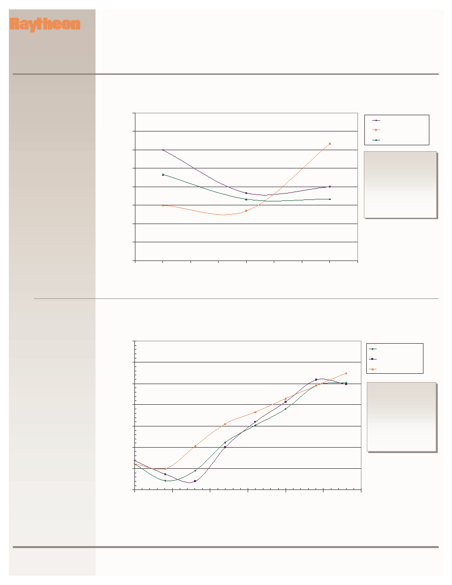
Single-Tone Output Power, Gain and
Power-Added Efficiency
0.0
5.0
10.0
15.0
20.0
25.0
30.0
35.0
40.0
45.0
-15.0
-12.5
-10.0
-7.5
-5.0
-2.5
0.0
2.5
5.0
7.5
Input P o we r (dB m)
P
o
w
e
r
(
d
B
m
)
,
G
a
i
n
(
d
B
),
E
f
fi
c
i
e
n
c
y
(%
)
Output Power
Power Gain
Power-Added
Efficiency
Tested at:
!
Vcc=3.5V
!
Vref=2.7V
!
f=1880
MHz
!
Tc=+25∞C
15.00
17.50
20.00
22.50
25.00
27.50
30.00
0.00
5.00
10.00
15.00
20.00
25.00
30.00
Output Pow er (dBm)
Gai
n
(
d
B
)
Tc= +25 deg C
Tc= -30 deg C
Tc= +85 deg C
CMDA Gain vs Output Power
Tested at:
!
Vcc=3.5V
!
Vref=2.7V
!
f=1880 MHz
!
Pout < 29 dBm
Performance
Data
Figure 5
Figure 6
Raytheon RF Components
362 Lowell Street
Andover, MA 01810
Revised February 6, 2003
Page 7
www.raytheonrf.com
Specifications are based on most current or latest revision.
PRODUCT INFORMATION
RMPA1951-102
3V PCS CDMA Power Amplifier Module
RF Components
-51.50
-51.00
-50.50
-50.00
-49.50
-49.00
-48.50
-48.00
-47.50
1840
1850
1860
1870
1880
1890
1900
1910
1920
Frequency (MHz)
ACPR1
(
d
Bc)
ACPR1_28_1
ACPR1_28_2
ACPR1_28_3
Tested at:
!
Vcc=3.5V
!
Vref=2.7V
!
Pout=+28 dBm
!
Offset= ±1.25 MHz
!
Tc=+25∞C
ACPR vs Frequency (3 Devices)
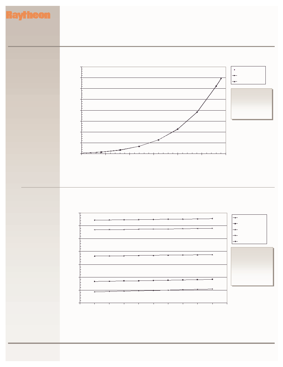
ACPR vs Output Power and Temperature
-75.00
-70.00
-65.00
-60.00
-55.00
-50.00
-45.00
-40.00
0.00
5.00
10.00
15.00
20.00
25.00
30.00
Output Power (dBm)
AC
P
R
1
(
d
B
c)
Tc=+25 deg C
Tc=-30 deg C
Tc=+85 deg C
Tested at:
!
Vcc=3.5V
!
Vref=2.7V
!
f=1880 MHz
!
Offset= ±1.25
MHz
!
Pout < 28 dBm
Figure 7
Figure 8
Raytheon RF Components
362 Lowell Street
Andover, MA 01810
Revised February 6, 2003
Page 8
www.raytheonrf.com
Specifications are based on most current or latest revision.
PRODUCT INFORMATION
RMPA1951-102
3V PCS CDMA Power Amplifier Module
RF Components
0.00
5.00
10.00
15.00
20.00
25.00
30.00
35.00
40.00
0.00
5.00
10.00
15.00
20.00
25.00
30.00
Output Power (dBm)
E
ffi
c
i
e
n
c
y
(%
)
Tc= +25 deg C
Tc=-30 deg C
Tc=+85 deg C
PAE vs Output Power and Temperature
Tested at:
!
Vcc=3.5V
!
Vref=2.7V
!
F=1880 MHz
DC Collector Current vs Output Power and Reference Voltage
0
100
200
300
400
500
600
700
2.60
2.65
2.70
2.75
2.80
2.85
2.90
2.95
3.00
3.05
3.10
Reference Voltage, Vref (V)
C
o
lle
c
t
or
C
u
r
r
e
n
t
,
Ic
c
(
m
A
)
Pout=+4 dBm
Pout=+16 dBm
Pout=+24 dBm
Pout=+28 dBm
Pout=+29 dBm
Tested at:
!
Vcc=3.5V
!
Vref=2.65 ≠
3.05V
!
F=1880 MHz
!
Tc = +25∞C
Figure 9
Figure 10
Raytheon RF Components
362 Lowell Street
Andover, MA 01810
Revised February 6, 2003
Page 9
www.raytheonrf.com
Specifications are based on most current or latest revision.
PRODUCT INFORMATION
RMPA1951-102
3V PCS CDMA Power Amplifier Module
RF Components
DC Power
Management
for Reduced-
Power Operating
Modes
Many Cellular/PCS handsets can benefit from gain control and DC power management to optimize
transmitter performance while operating at backed-off output power levels. Oftentimes, cellular systems
will operate at 10-20 dB back-off from maximum-rated linear power and peak power-added efficiency.
The ability to reduce current consumption under these conditions, without sacrificing linearity, is critical
to extending battery life in next-generation handheld phones.
The RMPA1951-102 PA offers the ability to lower quiescent current by more than 60 percent and small-
signal gain by up to 10 dB using a single control voltage (Vref). Even with the amplifier biased for lowest
current consumption, high linearity is maintained over the full operating temperature range and at output
power levels up to +16 dBm. Bias and gain control through Vref provides complete flexibility for the
handset designer, allowing the user to define the operation by either an analog (continuously-variable)
or digital (discrete-step) voltage input. As an example, reducing the Vref voltage from 2.7V (nominal) to
1.7V (minimum) can lower PA current consumption by more than 20 percent at an output power of +16
dBm.
The following charts demonstrate analog and digital control techniques for minimizing DC power
consumption at reduced RF output power levels. Figures 11 through 19 characterize analog control
over a reference voltage (Vref) range of 1.7V to 2.7V. Quiescent current is reduced to less than 30 mA
and small-signal gain is reduced by 10 dB at Vref=1.7V. Operating current at +16 dBm is also reduced
by 20 percent, or 35 mA, at the lowest reference voltage. Figures 20 through 23 feature digital control
using three discrete voltage levels (2.7V, 2.0V, 1.7V) to optimize linear PA performance over three
output power ranges (< +4 dBm, +4 dBm to +16 dBm, >+16 dBm). Alternate output power ranges can
be selected depending on the power-probability use in the cellular system.
Parameter
Symbol
Min
Typical
Max
Units
Conditions
Low-Power Range
P04
+4
dBm
Vref=1.7V typ
Current
Icc4
55
mA
Gain
G4
12.5
dB
Linearity
ACPR4
-50
dBc
Mid-Power Range
P16
+4
+10
+16
dBm
Vref=2.0V typ
Current
Icc16
160
mA
Gain
G16
20
dB
Linearity
ACPR16
-50
dBc
High-Power Range
P28
+16
+28
dBm
Vref=2.7V typ
Current
Icc28
560
640
mA
Pout=+28 dBm
Gain
G28
26
dB
Linearity
ACPR28
-50
dBc
DC Power
Management
Application of Digital
Control Technique

Raytheon RF Components
362 Lowell Street
Andover, MA 01810
Revised February 6, 2003
Page 10
www.raytheonrf.com
Specifications are based on most current or latest revision.
PRODUCT INFORMATION
RMPA1951-102
3V PCS CDMA Power Amplifier Module
RF Components
5.0
5.5
6.0
6.5
7.0
7.5
8.0
8.5
9.0
1.7
1.8
1.9
2.0
2.1
2.2
2.3
2.4
2.5
2.6
2.7
Vref (V)
P
o
w
e
r
-
A
d
d
e
d
E
f
f
ic
ie
n
c
y
(
%
)
PAE (+16 dBm)
0.0
10.0
20.0
30.0
40.0
50.0
60.0
70.0
80.0
90.0
100.0
1.7
1.8
1.9
2.0
2.1
2.2
2.3
2.4
2.5
2.6
2.7
Vref (V)
DC
Cu
r
r
e
n
t
(
m
A)
Iccq+Iref
Enhanced PAE vs Reference Voltage at Pout=+16 dBm (Analog
Control)
Total Quiescent Current vs Reference Voltage (Analog
Control)
Tested at:
!
Vcc=3.5V
!
Tc = +25∞C
Tested at:
!
Vcc=3.5V
!
F=1880 MHz
!
Tc = +25∞C
Figure 11
Figure 12

Raytheon RF Components
362 Lowell Street
Andover, MA 01810
Revised February 6, 2003
Page 11
www.raytheonrf.com
Specifications are based on most current or latest revision.
PRODUCT INFORMATION
RMPA1951-102
3V PCS CDMA Power Amplifier Module
RF Components
Small-Signal Gain (Pout=0 dBm) vs Reference Voltage (Analog
Control)
Total Current (ICC + Iref) vs Output Power and Reference
Voltage (Analog Control)
10.0
12.5
15.0
17.5
20.0
22.5
25.0
27.5
1.7
1.8
1.9
2.0
2.1
2.2
2.3
2.4
2.5
2.6
2.7
Vref (V)
S
m
a
ll-S
i
g
n
al
G
a
in
(d
B
)
SS gain
35.0
45.0
55.0
65.0
75.0
85.0
95.0
105.0
115.0
125.0
135.0
145.0
155.0
165.0
175.0
185.0
0.0
2.0
4.0
6.0
8.0
10.0
12.0
14.0
16.0
Output Power (dBm)
Ic
c
+
Ire
f
(
m
A
)
Vref=2.0V
Vref=1.9V
Vref=1.8V
Vref=1.7V
Vref=2.7V
Tested at:
!
Vcc=3.5V
!
F=1880 MHz
!
Tc = +25∞C
Tested at:
!
Vcc=3.5V
!
F=1880
MHz
!
Tc = +25∞C
Figure 13
Figure 14

Raytheon RF Components
362 Lowell Street
Andover, MA 01810
Revised February 6, 2003
Page 12
www.raytheonrf.com
Specifications are based on most current or latest revision.
PRODUCT INFORMATION
RMPA1951-102
3V PCS CDMA Power Amplifier Module
RF Components
10.0
12.5
15.0
17.5
20.0
22.5
25.0
27.5
0.0
2.0
4.0
6.0
8.0
10.0
12.0
14.0
16.0
Output Power (dBm)
Ga
i
n
(
d
B)
Vref=2.0V
Vref=1.9V
Vref=1.8V
Vref=1.7V
Vref=2.7V
Gain at +25∞C vs Output Power and Reference
Voltage (Analog Control)
Low-Power Mode
Gain vs Output Power and Temperature (Analog
Control)
10.0
12.5
15.0
17.5
20.0
22.5
0.0
2.0
4.0
6.0
8.0
10.0
12.0
14.0
16.0
Output Power (dBm)
Ga
i
n
(
d
B
)
Vref=2.0V (Tc=+25 deg C)
Vref=2.0V Tc=+85 deg C)
Vref=1.7V (Tc=+25 deg C)
Vref=1.7V (Tc=+85 deg C)
Tested at:
!
Vcc=3.5V
!
F=1880 MHz
Tested at:
!
Vcc=3.5V
!
F=1880 MHz
!
Tc = +25∞C
Figure 15
Figure 16
Raytheon RF Components
362 Lowell Street
Andover, MA 01810
Revised February 6, 2003
Page 13
www.raytheonrf.com
Specifications are based on most current or latest revision.
PRODUCT INFORMATION
RMPA1951-102
3V PCS CDMA Power Amplifier Module
RF Components
-55.0
-54.0
-53.0
-52.0
-51.0
-50.0
-49.0
-48.0
-47.0
-46.0
-45.0
0.0
2.0
4.0
6.0
8.0
10.0
12.0
14.0
16.0
Output Pow er (dBm)
A
C
P
R
1
a
t
+
/-
1.25
M
H
z
O
ff
set
(d
B
c
)
Vref=2.0V
Vref=1.9V
Vref=1.8V
Vref=1.7V
-55.0
-54.0
-53.0
-52.0
-51.0
-50.0
-49.0
-48.0
-47.0
-46.0
-45.0
0.0
2.0
4.0
6.0
8.0
10.0
12.0
14.0
16.0
Output Power (dBm)
ACPR1
a
t
+
/
-
1
.
2
5
M
H
z
O
f
f
s
e
t
(
d
Bc
)
Vref=2.0V
Vref=1.9V
Vref=1.8V
Vref=1.7V
Low-Power Mode - ACPR at +25∞C vs Output Power
and Vref (Analog Control)
Low-Power Mode - ACPR vs Output Power and Vref at
85∞C (Analog Control)
Tested at:
!
Vcc=3.5V
!
F=1880 MHz
!
Tc = +85∞C
Tested at:
!
Vcc=3.5V
!
F=1880 MHz
!
Tc = +25∞C
Figure 17
Figure 18
Raytheon RF Components
362 Lowell Street
Andover, MA 01810
Revised February 6, 2003
Page 14
www.raytheonrf.com
Specifications are based on most current or latest revision.
PRODUCT INFORMATION
RMPA1951-102
3V PCS CDMA Power Amplifier Module
RF Components
Low-Power Mode - ACPR vs Output Power and Temperature
(Analog Control)
-55.0
-54.0
-53.0
-52.0
-51.0
-50.0
-49.0
-48.0
-47.0
-46.0
-45.0
0.0
2.0
4.0
6.0
8.0
10.0
12.0
14.0
16.0
Output Power (dBm)
A
C
P
R
1
a
t
+
/-
1.
25
M
H
z
O
f
f
set
(
d
B
c
)
Tc=+25 deg C
Tc=+85 deg C
Vref=2.0V
Tested at:
!
Vcc=3.5V
!
Vref=2.0V
!
F=1880 MHz
Collector Current vs Output Power at +25∞C (Digital Control)
0
50
100
150
200
250
300
350
400
450
500
550
600
-20.0
-16.0
-12.0
-8.0
-4.0
0.0
4.0
8.0
12.0
16.0
20.0
24.0
28.0
Output Power (dBm)
Col
l
e
cto
r
Curre
n
t
(mA)
Vref=2.7V
Adj Vref
Vref=2.7V
Vref=1.7V
Vref=2.0V
Vref=2.7V
(Low-Power)
(High-Power)
(Mid-Power)
Tested at:
!
Vcc=3.5V
!
F=1880 MHz
!
Tc = +25∞C
Figure 19
Figure 20
Raytheon RF Components
362 Lowell Street
Andover, MA 01810
Revised February 6, 2003
Page 15
www.raytheonrf.com
Specifications are based on most current or latest revision.
PRODUCT INFORMATION
RMPA1951-102
3V PCS CDMA Power Amplifier Module
RF Components
Collector Current vs Output Power (Pout
+16 dBm) at +25∞C (Digital Control)
Vref=2.0V
Vref=1.7V
0
20
40
60
80
100
120
140
160
180
-20.0
-16.0
-12.0
-8.0
-4.0
0.0
4.0
8.0
12.0
16.0
Output Power (dBm)
C
o
l
l
e
c
t
o
r
C
urre
nt
(
m
A
)
Vref=2.7V
Adj Vref
Vref=2.7V
Vref=2.7V
(Low-Power)
(Mid-Power)
Tested at:
!
Vcc=3.5V
!
F=1880 MHz
!
Tc = +25∞C
Gain vs Output Power (Pout
+28 dBm) at +25∞C (Digital Control)
0.0
2.5
5.0
7.5
10.0
12.5
15.0
17.5
20.0
22.5
25.0
27.5
30.0
-20.0
-16.0
-12.0
-8.0
-4.0
0.0
4.0
8.0
12.0
16.0
20.0
24.0
28.0
Output Power (dBm)
Ga
i
n
(
d
B
)
Vref=2.7V
Adj Vref
Vref=2.7V
Vref=1.7V
Vref=2.0V
(Mid-Power)
(High-Power)
(Low-Power)
Vref=2.7V
Tested at:
!
Vcc=3.5V
!
F=1880 MHz
!
Tc = +25∞C
Figure 21
Figure 22

Raytheon RF Components
362 Lowell Street
Andover, MA 01810
Revised February 6, 2003
Page 16
www.raytheonrf.com
Specifications are based on most current or latest revision.
PRODUCT INFORMATION
RMPA1951-102
3V PCS CDMA Power Amplifier Module
RF Components
ACPR vs Output Power
(Pout
+28 dBm) at +25∞C (Digital Control)
-75.00
-72.50
-70.00
-67.50
-65.00
-62.50
-60.00
-57.50
-55.00
-52.50
-50.00
-47.50
-45.00
-20.0 -16.0 -12.0 -8.0
-4.0
0.0
4.0
8.0
12.0
16.0
20.0
24.0
28.0
Output Power (dBm)
ACP
R1
a
t
+
/
-
1
.
2
5
M
Hz
O
f
f
s
e
t
(
d
Bc
)
Vref=2.7V
Adj Vref
Vref=2.0V
Vref=1.7V
Vref=2.7V
Vref=2.7V
(Low-Power)
(Mid-Power)
(High-Power)
Tested at:
!
Vcc=3.5V
!
F=1880
MHz
!
Tc = +25∞C
Noise Figure vs Frequency (3 Devices)
2.00
2.50
3.00
3.50
4.00
4.50
5.00
5.50
6.00
6.50
7.00
1830
1850
1870
1890
1910
1930
1950
1970
1990
2010
Frequency (MHz)
No
is
e
F
ig
u
r
e
(
d
B
)
Unit 1_2.7V
Unit 2_2.7V
Unit 3_2.7V
Tested at:
!
Vcc=3.5V
!
Vref = 2.7
!
Tc = +25∞C
Figure 23
Figure 24